Skip to content
- Akito Suzuki, Takefumi Kamioka, Yoshinari Kamakura, Kenji Ohmori, Keisaku Yamada, and Takanobu Watanabe, “Source-induced RDF Overwhelms RTN in Nanowire Transistor: Statistical Analysis with Full Device EMC/MD Simulation,” IEEE International Electron Devices Meeting (IEDM 2014), Hilton San Francisco Union Square, San Francisco, USA, Dec. 14, 2014.
- Suichiro Hashimoto, Hiroki Kosugiyama, Kohei Takei, Jing Sun R. Imai, H. Tokutake, Motohiro Tomita, Atsushi Ogura, Takashi Matsukawa Meishoku Masahara and Takanobu Watanabe, “Impact of post-oxidation annealing of Si nanowire on its Ni silicidation rate,” 27th International Microprocesses and Nanotechnology Conference (MNC 2014), Hilton Fukuoak Sea Hawk, Fukuoka, Japan, Nov. 6, 2014.
- (Invited) Takanobu Watanabe, Ryo Kuriyama, Masahiro Hashiguchi, Ryusuke Takahashi, Kosuke Shimura, Atsushi Ogura, and Sinich Satoh, “Molecular Dynamics Simulation of Dipole Layer Formation at High-k/SiO2 Interface,” 226th Meeting of The Electrochemical Society, Moon Palace Resort, Cancun, Mexico Oct. 6, 2014.
- Tomofumi Zushi, Kenji Ohmori, Keisaku Yamada, and Takanobu Watanabe, ” Thermal Transport Properties of Si Nanowire Covered with SiO2 Layer: A Molecular Dynamics Study,” 2014 International Conference on Solid State Devices and Materials (SSDM 2014), Epocal Tsukuba, Tsukuba, Japan, Sep. 10, 2014.
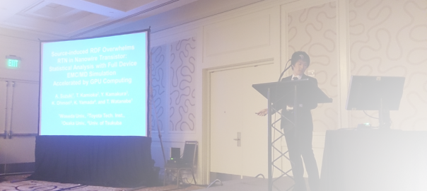
- Akito Suzuki, Takefumi Kamioka, Yoshinari Kamakura, and Takanobu Watanabe, “Full-Scale Whole Device EMC/MD Simulation of Si Nanowire Transistor Including Source and Drain Regions by Utilizing Graphic Processing Units,” 2014 International Conference on Simulation of Semiconductor Processes and Devices (SISPAD 2014),” Mielparque Yokohama, Yokohama, Japan, Sep. 11, 2014.
- (Requested) Takanobu Watanabe, “Molecular dynamics simulation of gate dielectric thin films,” The 5th NIMS/MANA-Waseda University International Symposium, NIMS Sengen site, Tsukuba, Japan, Mar. 24, 2014.
- Tomofumi Zushi, “A Simulation Study of Thermoelectric Properties of Silicon Nanotubes,” The 5th NIMS/MANA-Waseda University International Symposium, NIMS Sengen site, Tsukuba, Japan, Mar. 24, 2014.
- Ryo Kuriyama, Masahiro Hashiguchi, Ryusuke Takahashi, Atsushi Ogura, Shinichi Satoh, Takanobu Watanabe, “Molecular Dynamics Study on the Formation of Dipole Layer at High-k/SiO2 Interfaces,” 2013 International Workshop on DIELECTRIC THIN FILMS FOR FUTURE ELECTRON DEVICES – SCIENCE AND TECHNOLOGY -, University of Tsukuba (Tokyo Campus), Tokyo, Japan, Nov. 7, 2013.
- Hiroki Yamashita, Hiroki Kosugiyama, Yasuhiro Shikahama, Shuichiro Hashimoto, Kouhei Takei , Jing Sun, Takashi Matsukawa, Meishoku Masahara, and Takanobu Watanabe, ” 26th International Microprocesses and Nanotechnology Conference (MNC 2013), Royton Sapporo, Sapporo, Japan, Nov. 7, 2013.
- Kotaro Mura, Takefumi Kamioka, Tetsu Kitani, Kenta Imazu, and Takanobu Watanabe, “Real-time Scanning Tunneling Microscopy Observation of Ni Ion Irradiation Process on Si(111) Surfaces,” 12th International Conference on Atomically Controlled Surfaces, Interfaces and Nanostructures (ACSIN-12), Tsukuba International Congress Center, Tsukuba, Japan, Nov. 5, 2013.
Warning: Undefined array key "sfsi_facebook_display" in /home/watanabelab/watanabe-lab.jp/public_html/wp-content/plugins/ultimate-social-media-icons/libs/controllers/sfsiocns_OnPosts.php on line 450